- 您现在的位置:买卖IC网 > Sheet目录1994 > DS3106LN+ (Maxim Integrated Products)IC TIMING LINE CARD 64-LQFP
DS3106
10
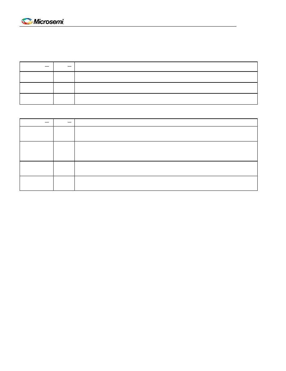
6. Pin Descriptions
Table 6-1. Input Clock Pin Descriptions
PIN NAME
TYPE
PIN DESCRIPTION
REFCLK
I
Reference Clock. Connect to a 12.800MHz, high-accuracy, high-stability, low-noise local
oscillator (XO or TCXO). See Section 7.3.
IC3
IPD
Input Clock 3. CMOS/TTL. Programmable frequency. Default frequency selected by IPF[2:0]
pins when the
RST pin goes high, 8kHz if IPF[2:0] pins left open.
IC4
IPD
Input Clock 4. CMOS/TTL. Programmable frequency. Default frequency selected by IPF[2:0]
pins when the
RST pin goes high, 8kHz if IPF[2:0] pins left open.
Table 6-2. Output Clock Pin Descriptions
PIN NAME
TYPE
PIN DESCRIPTION
OC3
O
Output Clock 3. CMOS/TTL. Programmable frequency. Default frequency selected by
O3F[2:0] pins when the
RST pin goes high, 19.44MHz if O3F[2:0] pins left open. See Table
OC6POS,
OC6NEG
ODIFF
Output Clock 6. LVDS/LVPECL. Programmable frequency. Default frequency selected by
O6F[2:0] pins when the
RST pin goes high, 38.88MHz if O6F[2:0] pins left open. The output
FSYNC
O3
8kHz FSYNC. CMOS/TTL. 8kHz frame sync or clock (default 50% duty cycle clock,
noninverted). The pulse polarity and width are selectable using FSCR1.8KINV and
FSCR1.8KPUL.
MFSYNC
O3
2kHz MFSYNC. CMOS/TTL. 2kHz frame sync or clock (default 50% duty cycle clock,
noninverted). The pulse polarity and width are selectable using FSCR1.2KINV and
FSCR1.2KPUL.
发布紧急采购,3分钟左右您将得到回复。
相关PDF资料
DS3231MZ+
IC RTC I2C 8SOIC
DS3231SN#T&R
IC RTC W/TCXO 16-SOIC
DS3232MZ+
IC RTC W/SRAM I2C 8SOIC
DS3232SN#T&R
IC RTC W/TCXO 20-SOIC
DS3234S#
IC RTC W/TCXO 20-SOIC
DS32C35-33#T&R
IC RTC ACCURATE I2C 3.3V 20-SOIC
DS3911T+
IC DAC 10BIT I2C QUAD 14TDFN
DS4000KI/WBGA
IC OSC TCXO 19.44MHZ 24-BGA
相关代理商/技术参数
DS3107FP000
制造商:Thomas & Betts 功能描述:30A,CON,2P3W,MG,107,125V
DS3107FRAB0
制造商:Thomas & Betts 功能描述:30A,REC,2P3W,MG,107,AB0,125,SC
DS3107MP000
制造商:Thomas & Betts 功能描述:30A,PLG,2P3W,MG,107,125V
DS3107MP00K
制造商:Thomas & Betts 功能描述:30A,PLG,2P3W,MG,107,125V,CC
DS3107MR000
制造商:Thomas & Betts 功能描述:30A,NLT,2P3W,MG,107,125V
DS3107MRAB0
制造商:Thomas & Betts 功能描述:30A,NLT,2P3W,MG,107,AB0,125V
DS3108A14S5S621
制造商:Amphenol Corporation 功能描述:
DS3108A14S6S
制造商:Amphenol Corporation 功能描述: